Foundry capacity limitations: AI chip supply constraints
Analyze the foundry capacity limits constraining AI chip supply, from TSMC CoWoS packaging bottlenecks and HBM shortages to US export controls.
In this article8
The physical limits of AI chip production
The bottleneck in artificial intelligence hardware has transitioned from logic design complexity to physical semiconductor manufacturing constraints. While architecture advancements enable higher theoretical floating-point operations, delivery volume depends on wafer fabrication throughput and advanced packaging capacity. Leading-edge logic is booked far ahead: TSMC's N2/A16 capacity is reported booked into 2028 with lead times of 78 to 156 weeks, while N3 runs tight at 52 to 78 weeks, and only N7 and mature nodes remain broadly available[1].
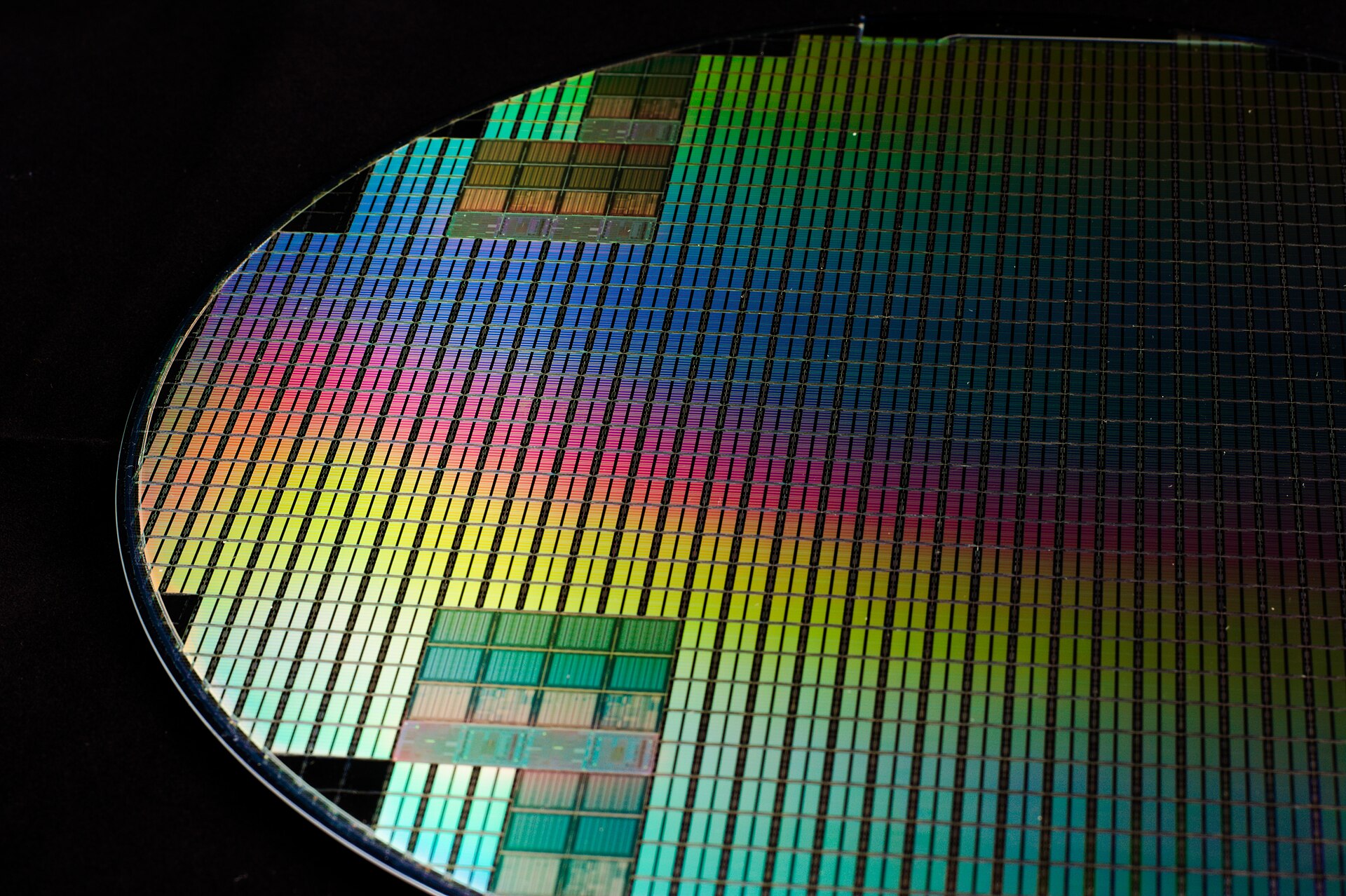
Leading-edge AI accelerators differ from standard server processors due to their massive silicon footprints, often approaching or exceeding the reticle limit (roughly 858 mm²). Fabricating monolithic dies of this scale results in lower yields per wafer, compounding wafer utilization challenges across premier contract foundries fabrication. Consequently, the physical bounding factor in hardware deployment is not solely raw silicon starts, but the yield-loss curves and multi-chip assembly capacity required to construct modular systems.
| Manufacturing Stage | Primary Limiting Factor | Supply Chain Impact |
|---|---|---|
| Leading-Edge Front-End | Extreme ultraviolet (EUV) tool availability and reticle area constraints | Restricted wafer starts at 3nm and 2nm nodes |
| Interposer Fabrication | Large-area silicon interposer yield and lithography stitching | Limits total compute-memory bridge substrates |
| Heterogeneous Integration | Multi-die placement precision and thermal dissipation bonding | Determines final accelerator module throughput |
Because AI processors require large silicon surfaces and low-latency communication between compute logic and memory stacks, production scaling depends directly on back-end packaging lines rather than traditional front-end lithography lines alone.
Where the packaging queue caps accelerator volume
Taiwan Semiconductor Manufacturing Company (TSMC) operates the industry-standard packaging architecture for modern accelerators: Chip-on-Wafer-on-Substrate (CoWoS). CoWoS integrates logic dies and memory stacks onto a passive silicon or redistribution-layer interposer, providing thousands of high-density interconnect wires. TSMC keeps expanding monthly CoWoS output, yet both the CoWoS-S and CoWoS-L families are reported fully booked, with lead times running between 52 and 78 weeks[1].
- Allocation concentration: A single primary accelerator vendor commands over 50 percent of total global CoWoS allocation, leaving competing designers and sovereign cloud initiatives constrained.
- Substrate sizing: Modern designs (such as CoWoS-L) utilize interposers up to 3.3 times the reticle size, reducing the total number of accelerator modules yieldable per wafer.
- Tooling lead times: Equipment for wafer-level bonding and high-precision die placement requires 12 to 18 months from order placement to operational fab floor integration.
The structural concentration of CoWoS lines in Taiwan introduces geographic supply bottlenecks. Even when raw wafer slicing and etching proceed on schedule, logic dies must wait in packaging queues before final assembly, creating persistent hardware backlogs that impact global accelerator pricing and delivery schedules.
High-Bandwidth Memory constraints
AI accelerators cannot operate without dense, high-throughput memory subsystems. High-Bandwidth Memory (HBM3e and HBM4) stacks several dynamic random-access memory (DRAM) dies vertically using through-silicon vias (TSVs). The physical integration of HBM with compute logic introduces a secondary, parallel supply choke point.
- TSV fabrication overhead: Etching microscopic vertical channels across 8 to 16 stacked DRAM dies increases manufacturing cycle times compared to standard DDR5 memory.
- Thermal and mechanical stress: Warpage during high-temperature thermal compression bonding reduces packaging yields across large-area interposers.
- Compound scrap risk: If a single DRAM die within a 12-high HBM stack fails during final packaging, the entire multi-chip accelerator module is scrapped.
The mandatory pairing of HBM with compute logic tightly couples memory fabrication to foundry packaging capacity. Saturated packaging lines delay the integration of available DRAM, while spot shortages in high-grade HBM wafers halt finished accelerator validation lines, amplifying supply unpredictability.
How regulation narrows accessible capacity
Capacity that exists is not always capacity a given buyer can access, because regulation governs where advanced logic may ship. The United States Department of Commerce Bureau of Industry and Security (BIS) maintains controls over advanced computing integrated circuits and semiconductor manufacturing equipment, and publishes consolidated guidance on those rules[2]. The detail of those rules is covered separately in our dedicated write-up on US export controls; here the point is only how they shift effective supply.
- May 13, 2025 policy updates: BIS published updated guidance and a policy statement on advanced computing integrated circuits and the commodities used to train AI models[3].
- Interconnect and performance thresholds: Export restrictions regulate total processing performance (TPP) and interconnect bandwidth density, altering die design parameters for non-restricted markets[2].
- Foundry licensing requirements: The Foreign-Direct Product Rules extend the Export Administration Regulations to foreign-produced advanced computing items made with US-origin software, technology, or equipment, so foundries need a license before shipping such logic to designated entities[4].
These regulatory measures create secondary supply chain distortions. Foundries must allocate engineering and legal resources toward compliance verification, while international buyers face extended review periods when procuring equipment governed by export controls.
European R&D responses to semiconductor dependence
In response to global supply vulnerabilities, European research hubs and institutions are advancing regional capabilities in semiconductor design, pilot lines, and heterogeneous integration. Interuniversity Microelectronics Centre (imec) inaugurated a 2,000 m² cleanroom expansion in Leuven on 9 February 2026 for the NanoIC pilot line, part of the EU Chips Act push toward beyond-2nm systems-on-chip[5]. The expansion sits within a total imec cleanroom capacity of more than 12,000 m², with a further 4,000 m² cleanroom due to start construction[6].
- imec NanoIC pilot line: Provides open-access research infrastructure for advanced logic patterning, 3D system integration, and novel packaging materials across European industry partners[5].
- Fraunhofer microelectronics leadership: On 3 August 2026, Fraunhofer announced that Prof. Dr.-Ing. Wenke Weinreich assumed the co-leadership of the Fraunhofer Institute for Photonic Microsystems (IPMS), alongside her appointment at TU Dresden for Functionalized Microelectronics for Heterogeneous Systems[7].
- Heterogeneous packaging research: Development of chiplet architectures and silicon photonics to reduce reliance on single monolithic leading-edge wafer runs.
These European R&D initiatives focus on mid- to long-term technological sovereignty. While full domestic manufacturing parity for commercial 3nm volume remains years away, regional research creates critical intellectual property and pilot packaging techniques.
Securing AI compute amid prolonged scarcity
With physical lead times extending up to 78 weeks for enterprise accelerator shipments, organizations planning compute-heavy AI deployments face substantial operational delays. Hardware acquisition cycles require extensive capital allocation long before physical delivery occurs, exposing infrastructure plans to supply shifts and component delays across established infrastructure providers.
- Direct hardware procurement: Carries 52 to 78 weeks of delivery lead time, high upfront capital commitments, and allocation risk in foundry backlogs.
- Pre-secured GPU infrastructure: Eliminates component-level procurement delays by leveraging operational datacenter capacity with established hardware allocations.
For teams requiring rapid deployment without hardware procurement backlogs, Large-Scale GPU Cluster provides pre-secured GPU capacity through a European sourcing network of more than 40 partners. Around 200 GPUs is the largest single-customer deployment running today, and a 1,000-GPU deployment is in build. New hardware allocations maintain standard lead times around 4 weeks, with minimum reservations starting at one month and one server, enabling European enterprises to deploy dedicated compute capacity independently of multi-year foundry queues.
Frequently asked questions
What is causing the AI chip supply shortage?
The shortage is driven by physical manufacturing constraints rather than silicon wafer production. The primary bottleneck is advanced packaging capacity, specifically TSMC's CoWoS (Chip-on-Wafer-on-Substrate), which is required to integrate logic dies with High-Bandwidth Memory (HBM).
How long are the lead times for AI accelerators?
Lead times for leading AI accelerators are reported at 52 to 78 weeks. This prolonged delay is a structural constraint caused by fully booked advanced packaging lines at foundries, forcing enterprises to rely on alternative compute procurement strategies.
Why is CoWoS packaging capacity fully booked?
CoWoS enables high-density integration of processors and memory, and every leading accelerator needs a slot. TSMC keeps expanding monthly capacity, but bookings are placed well in advance, so both CoWoS-S and CoWoS-L lines remain fully allocated even as output grows.
How does regulation change the capacity a buyer can access?
The US Bureau of Industry and Security (BIS) enforces export rules on advanced computing integrated circuits, which determine which regions and entities can procure top-tier AI chips. The practical effect is that global capacity and accessible capacity are not the same number for a given buyer.
How is Europe responding to semiconductor supply limits?
Europe is investing in sovereign manufacturing and R&D capabilities under the EU Chips Act. This includes the NanoIC pilot line at imec, where a 2,000 square metre cleanroom expansion opened in February 2026 within a total cleanroom footprint of more than 12,000 square metres, plus advanced microelectronics research for heterogeneous systems at Fraunhofer IPMS.
Sources
- TSMC Foundry Allocation 2026: CoWoS Sold Out, 2nm Booked siliconanalysts.com
- Bis updated public information page export controls imposed advanced computing semiconductor bis.gov
- bis.gov
- Foreign-Produced Direct Product Rule Additions, and Refinements to Controls for Advanced Computing and… federalregister.gov
- Imec inaugurates NanoIC pilot line imec-int.com
- EU launches NanoIC, Europe’s largest Chips Act pilot line evertiq.com
- Fraunhofer IPMS Appoints Wenke Weinreich as Second Director fraunhofer.de
Rankings and scores on Optinest cannot be bought — no commercial relationship changes how a provider is assessed. How we score
Related reading
All Fabrication →Packaging, not fabs, is the chip bottleneck
An analysis of the advanced packaging bottleneck restricting AI chip supply, featuring CoWoS capacity data, BIS export controls, and compute procurement

US chip export controls reach European buyers
Understand how US export controls on AI chips impact EU buyers. Learn the compliance obligations and how European capacity mitigates supply chain exposure.

US entity list China semiconductor: AI chip export controls
US entity list China semiconductor: what a designation requires of a buyer, which rule text carries it (15 CFR 744.11), and where to check.
